Our Interests
Semiconductor Nanostructures
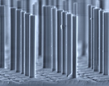
Nanostructures of semiconductor are of both fundamental and practical interest. We can explorer distinguished physical and chemical properties of nanostructured materials to bulk materials, which are associated with their low dimensionality and unusual physical phenomena such as the quantum confinement effect. Moreover, taking structural advantage of them, nanostructured semiconductor can be utilized as a building block of practical advanced devices. The manipulation of material structures and morphologies in nanoscale is the key idea to the evolution of high efficient devices for light-detecting, energy harvesting, sensing. We are now in the process of fabrication and characterization of nanostructured semiconductors (Si nanowires and ZnO nanopatterns) and 2-dimension materials (graphene quantum dots and nanoribbons).
Selected Papers
1. Sung Kim, Dong Hee Shin, and Suk-Ho Choi, “Ultrafast photoluminescence from freestanding Si nanocrystals”, Appl. Phys. Lett. 100, 253103 (2012).
2. S. Kim, S. W. Hwang, M.-K. Kim, D. Y. Shin, D. H. Shin, C. O. Kim, S. B. Yang, J. H. Park, E. Hwang, S.-H. Choi, G. Ko, S. Sim, C. Sone, H. J. Choi, S. Bae, B. H. Hong, “Anomalous behaviors of visible luminescence from graphene quantum dots: interplay between size and shape”, ACS Nano 6, 8203 (2012).
3. Jung Kil Kim, Suk-Ho Choi, Young-Hun Kim, and Woo Lee, “Curved Silicon Nanowires with Ribbon-Like Cross-Sections by Metal-Assisted Chemical Etching”, ACS Nano 5, 5242 (2011).
4. Jung Kil Kim, Hee Han, Young-Hun Kim, Suk-Ho Choi, Jae-Cheon, Kim, and Woo Lee, “Au/Ag bi-layered metal meshes as Si etching catalyst for controlled fabrication of Si nanowires”, ACS Nano 5, 3222 (2011).
5. S. Kim, C. O. Kim, D. H. Shin, S. H. Hong, M. C. Kim, J. Kim, S.-H. Choi, T. Kim, R. G. Elliman, Y.-M. Kim, “Self-assembled growth and luminescence of crystalline Si/SiOx core-shell nanowires”, Nanotechnology 21, 205601 (2010).